Overview
As an aerospace engineering student with limited prior electronics experience, the PCB schematic, layout, and firmware on this project were entirely self-taught from learning KiCad and mixed-signal layout rules to writing embedded C drivers from scratch.
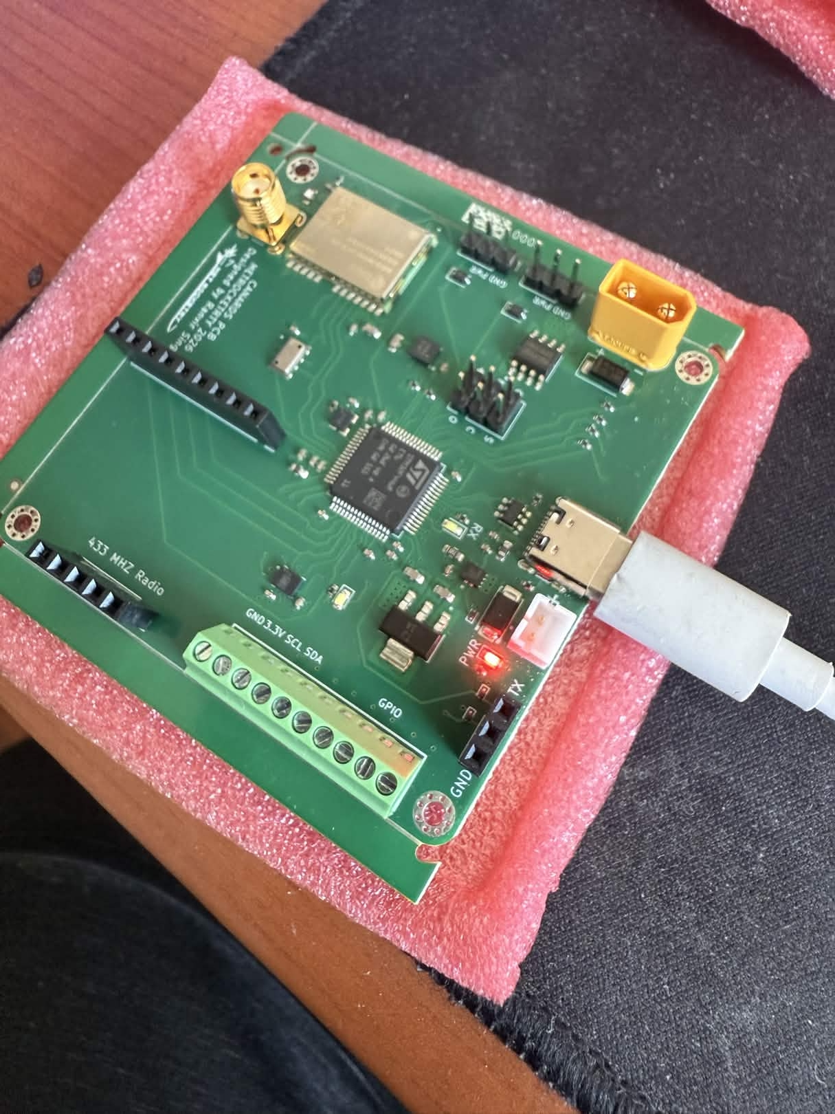
This flight computer was designed from the ground up to work for active control projects, containing a multiude of sensors for altitude, and Attitude estimation along with connection for servo motors for use with either canards or airbrakes. This PCB is an STM32F446RE based 4 layer PCB, the choice to go with an STM32 over other microcontrollers primarily had to do with the expanded debuging capability that ST microcontrollers bring over Arduino based controllers, additonally the vase user base meant there were many support guides and imformation for aiding development. The PCB contains an IMU, Barometer, Magnetometer, and a GPS along with a high side switch to cut power to the servos in emergencies. It also have connections for a Lora 443 MHZ radio for telemetry. The PCB originally started as just the flight controller for the canard control system but was then incorporated into our rockets AI vision tracking payload for data and telemtry (hense the radio).
The canard control PCB was programmed with a strong focus on reliability, modularity, and real-time performance. An RTOS was implemented to organize the software into dedicated tasks such as sensor polling, state estimation, control calculations, actuator commands, and data logging, ensuring time-sensitive functions were run in a structured manner. A watchdog timer was also integrated as a fault-recovery feature, automatically resetting the system if the firmware became unresponsive during operation. Additional features included sensor and peripheral communication drivers, flight-state logic, PWM-based servo actuation, onboard data logging, and fault-handling routines to improve robustness. Together, these software features ensured the PCB could support stable canard control while maintaining the reliability required for an embedded aerospace application.
Requirements
- Output accurate PWM signals for Servos
- Low latancy sensor data reading
- High frequency guidence and contro loop
- Low EMI and electrical noise
- Package and send telemetry info in structured and timly manner
Key design decisions
STM32F446RE over Arduino-based controllers
The STM32 was primarily chosen for its larger control over hardware, allowing for dirrect configuration of timers, interupts, the data lines and DMA. Additionally the debugging capability was far superior, providing breakpoints, live register inspection along with the many other tools that come with serial wire debuging.
4-layer stackup
A 4-layer board (signal / ground / power / signal) was selected to provide a continuous ground reference plane beneath all sensor traces, significantly reducing EMI and crosstalk compared to a 2-layer layout. The added cost was justified by the noise-sensitive IMU and barometer signals.
Separate 7.4 V servo rail
The servos selected were capable of running on voltages between 6-8.2V initial itterations attempted to use a buck-boost converter to run the servos at 8.2V to gain the small boost in torque but it was deemed an unnessecary complication and simply running staight off the 7.4V provided by a 2S li ion battery would be simpler and still provide adequate torque.
RTOS over bare-metal scheduling
An RTOS was chosen over a bare-metal super-loop to enforce deterministic timing across concurrent tasks and simplify adding or removing features without reworking the entire scheduling model.
System architecture
The PCB is centred on an STM32F446RE, with dedicated sensor, actuator, and telemetry buses managed by an RTOS.
RTOS Task Scheduler
Sensors (I²C / SPI)
Actuators (PWM)
Comms & Storage
Figure 2 — Flight computer block diagram showing MCU, RTOS tasks, sensors, actuators, and comms.
Schematic & layout
The schematic was drawn in KiCad, with separate sheets for power, MCU, sensors, and connectors. The 4-layer layout follows a signal / ground / power / signal stackup with pour zones and stitching vias isolating the servo power domain from the sensor domain.
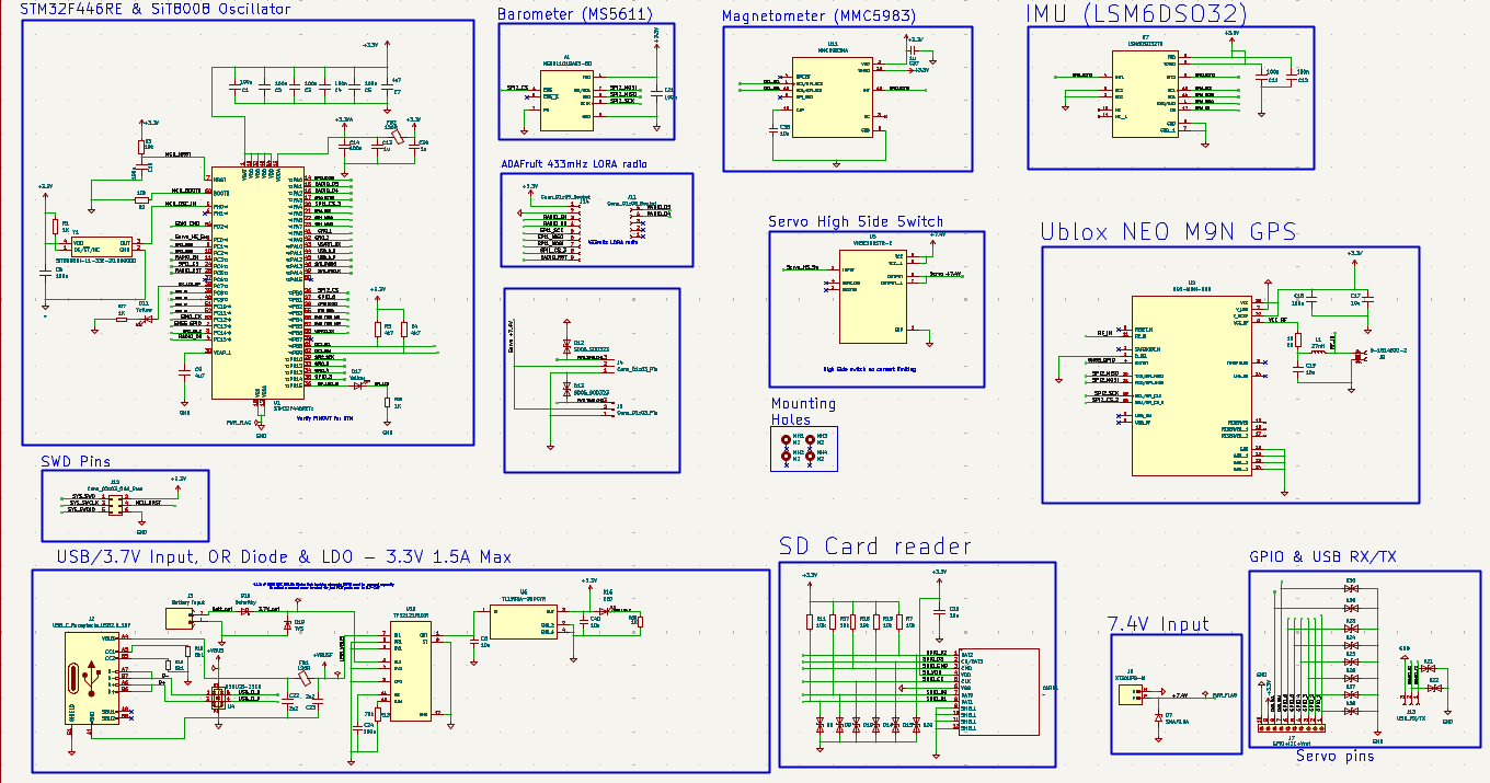
Figure 3 — Orion flight computer schematic
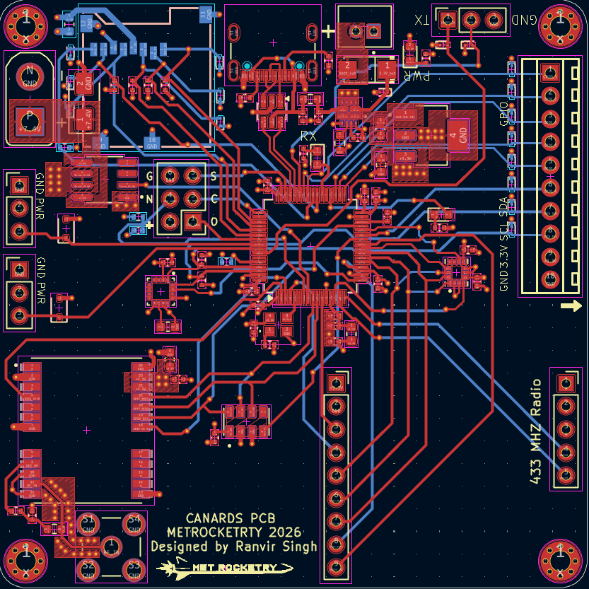
Figure 4 — Orion flight computer routing layout
Design & implementation
Initial design
The first version took approximately 3 weeks and contained numerous sub revisions due to new information being learned and also input from more experienced PCB designers. This version seeked to accomplish all the goals set out above but also recognized the likely hood of a mistake or design over sight occurring. Once the PCB was manufactured and received immediately issues were found, one of the most blatant flaws was the ESD diode packages used for the USB port was wired incorrectly, resulting in ground going to VCC and vice versa as a result the diode began to smoke and the USB lines did not work for that PCB, though power was still delivered due to the wiring method. The two other major flaws were first the external oscillator which was wired incorrectly and would not be usable meaning the internal oscillator would need to be used. The third major flaw came with the SD card which was also wired incorrectly. Additionally other ease of life issues also cropped up like the choice to go with micro USB rather than the more common USB-C and issues with wiring the serial wire debug pins for debug.
What works
- STM32 boots and enumerates all sensors over I²C and SPI
- 3.3 V regulator provides stable power under sensor load
- Sensors were able to return accurate data
- Radio and GPS were both able to be turned on and could send/recive data
- High side switch & 7.4V rail worked
What needs to change
- Ensure proper verification and validation, rereading of data sheets and wiring guides
- Additonal silkscreen needed for info/debug allowing other to also use the PCB
- Fix of USB ESD Diode wiring
- Add reverse polarity protection to 3.3V rail
- Fix the wiring issues with the Oscilator and SD card
- Change Micro USB port to USB C
- Add more I/O port and also break out a data line (I2C or SPI)
Revised design
Version 2 fixed many of the issue faced in version 1 and is the fligh board that will be used going forward for active control systems. The biggest change came from the verification and validation, an addequate amount of design time was spent making sure the data sheets were followed and check with more experienced individuals were also preformed. This verison also switched out the Inertial measurement unit due to shortages with the original one (BMI088 to ST LSM6DSO32). It aslo contained more information of the board itself making it easier for peopel to hook up the Serial wire debug pins without needing a schematic. The USB port was also switched to a USB-C port which made it much easier to connect to rather than the now hard to find micro USB. More imporovements were also made to traces and to ESD protection as I learned more in the time between the version, along with actual reverse polarity protection being provied to the 3.3 rail.
Future plans
- Validate LoRa telemetry link end-to-end with the ground station
- Conduct full hardware-in-the-loop (HIL) test of the control loop with live sensor data
- Characterise IMU noise floor and fine-tune Kalman filter covariance matrices
- Flight-test the board in a sub-scale rocket before the full canard flight
- Evaluate adding a secondary IMU for redundancy and cross-validation
Challenges
Mixed-signal noise
The 7.4 V servo rail introduced switching noise that corrupted IMU readings on V1. Solved in V2 by splitting the ground plane at the power entry point, adding stitching vias around the servo driver, and routing the sensor I²C lines away from high-current traces.
Real-time scheduling under tight loop budgets
Meeting the control loop deadline while simultaneously polling sensors, running the estimator, and logging to SD required careful RTOS task prioritisation. Sensor polling and actuator commands were given the highest priority; SD logging was deferred to a low-priority task with a ring buffer to prevent blocking.
LoRa footprint error
A pin-mapping mismatch between the chosen LoRa module and the KiCad footprint rendered the radio non-functional on V1. Identified through continuity testing and datasheet cross-referencing; the footprint was corrected and design rule checks were tightened for V2.
SD card signal integrity
SPI lines to the SD card showed ringing at higher clock speeds due to missing series termination. Added 33 Ω resistors on the CLK and MOSI lines in V2, which cleaned up the waveform and eliminated intermittent write failures.